Overview#
First if we take a look at the Relay computer designed by Harry Porter (from now on I’ll refer to it as the HP Design or HP Architecture).

It’s an excellent, elegant design. But in studying it and the subsequent refinements made by Paul Law and DipDot (https://www.youtube.com/@dipdoting) I started to wonder where else I could take it, and what I could add.
So let me introduce YARP - Yet Another Relay comPuter!

Specification#
The core of my design is based on the ‘HP architecture’ - if it ain’t broke don’t fix it! But I decided to make some fundamental changes.
12-Bits#
The computer is 12-bits. 12-bit Address bus, 12-bit Data bus and 12-bit ALU.
12-bit computers have their place in History. Besides who could not resist building a computer with 12 binary digits, or three nibbles (a ’tribble’)! Mr Spock would be proud!
Using a 12-bit data and address bus has given me the ability to enhance some of it’s core features and the room to extend it’s capabilities in the future. I settled on 12-bits as I thought is was the sweetspot (for me).
- I can play with large’ish numbers (4095 max).
- I can have a much larger instruction set.
- I’d never need more that 4096 ‘bytes’ of memory in reality - a 16 bit address range would be overkill as the majority of memory space would never be used.
- I don’t have to worry about High and Low register pairs such as the X and Y data registers in the HP architecture which becomes the XY address register.
NOTE: I’ll often refer to storing Bytes or grabbing the next Byte. Unless otherwise noted I’ll always be referring to a 12-Bit ‘Byte’. If such a thing exits!
As for the number of relay’s used - it will take more relays - but I don’t think the amount will be as significant as I first thought as I am increasing the data-bus but reducing the address bus across the design.
ALU Enhancements#
With the increase in Instruction set, I’ve also been able to increase the capabilities of the ALU. The ALU is now split into three separate functional areas (ALU_A, ALU_L and ALU_S) each having it’s own or multiple cards.
- ALU_A (Arithmetic) will be able to add, subtract, increment and decrement all in hardware. It will support B+C, B-C, INC_B, INC_C, DEC_B and DEC_C.
- ALU_L (Logic) will support all common logic gates ADD, OR, NAND, NOR, XOR, XNOR, NOT_B and NOT_C.
- ALU_S (Shift) will support Shift Left B, Shift Left C, Rotate Left B, Rotate Left C, and the same shifting to the Right. Shift Right B, Shift Right C, Rotate Right B, Rotate Right C.
Memory Stack and Interrupts#
I would like to implement an 8 byte stack. This will be able to hold the contents of ALL working registers and program counter. The instruction set will support PUSH, POP and PEEK to any register or the program counter.
I also have an Interrupt handling system planned. Servicing an interrupt will be achieved by switching between two different FETCH-NEXT cycles. The decision on what FETCH-NEXT cycle to use will be decided by the state of the INTERRUPT and INTERRUPT ENABLE lines.
In order to understand how the INTERRUPT FETCH-NEXT cycle works I should first explain how a normal FETCH-NEXT cycle works.
- You Read the memory at the address stored in the PC, this is loaded into the instruction register.
- While the PC is selected and the current address is on the address bus the Incrementor reads the address, adds one then stores it in the INC register.
- This new address (PC+1) that is stored in the INC register is then stored back in the PC.
If an Interrupt is triggered the INTERRUPT FETCH-NEXT cycle will be enabled. This will…
- Disable further interrupts by disabling the INT_EN line. This ensures you cannot interrupt an interrupt.
- PUSHes the current PC onto the Stack.
- Sets the PC to a predefined address (tbd). I might store this in it’s own interrupt address register, or hard code a default address - not sure yet).
- Continue loading the Instruction Register and incrementing the PC in the normal way as above (this time from the Interrupt address) completing the Fetch-Next cycle.
With this complete we are now running the interrupt service routine. The interrupt program code will…
- PUSH any other required registers onto the stack. If the Interrupt code only requires registers B and C then they are the only ones that need to be PUSH’ed.
- Execute the interrupt code.
To return back to the main program the interrupt service routine will…
- POP the working registers back to their original values.
- POP the PC back to it’s original value.
- Re-enable the INT_EN line.
The main program will then resume where it left off.
The Stack will be a large sub project on it’s own. I’ll need 8 memory locations, each one selected by a 3-8 line decoder.
- Each PUSH will increment a stack pointer then load the value on the data bus into that current location.
- Each PULL sets the value of the current stack location onto the data bus, then will decrement the stack pointer.
- Two condition flags Stack Empty, and Stack Overflow will be able to be tested as a JUMP condition in a similar way to SN, CY, EZ and NZ.
- I am toying with the idea of having a switch so that I can choose if a Stack Overflow will HALT the computer.
Increase the number of working registers#
My design will have more working registers than the ‘HP architecture’. I am still undecided about if these additional registers will be Data only such as the A,B,C or D registers or data and address registers such as X or Y. I might add some of each type.
Dedicated I/O Instructions#
I will have a dedicated I/O address bus (which will probably only be 4 bit - supporting 15 peripherals. To Read from an I/O address you will first set the I/O Address, then Read or Write.
Once the I/O address it set subsequent reads or writes will be to the same address.
The I/O interface has the ability to set the computer to WAIT until the I/O hardware is ready to return data. This will freeze the clock until the wait is cleared.
IOSET xxxx,dddd - Sets the IO address to use.
IOWRI nnnnnnnn - Writes an 8-bit value directly to the address set in IOSET.
IORD aaaa,dddd - Read IO at address aaaa and stores in register dddd.
IOWR ssss,aaaa - Write the value stored in register ssss to IO address.
Side projects#
No project would be complete without random side projects to burn the hours away. I am keeping to this tradition!
- Building some form of paper tape reader / writer (for 12-bit data!)
- A ‘ROM cartridge’ system. that I can use to store a bootloader.
- Custom case to make it ‘portable’ (but I’ll settle for luggable!). I want to be able to take this to maker fair’s and let people interact with it as much as possible. I’d like to go with a slightly WW2 / steampunk look. Bakelight and Brass!
- A true Random Number Generator. I’m imagining a marble drop machine with 12 channels at the bottom, when you ask for a random number it reads the colour of the balls (black or white) before re circulating them back up to be dropped again. Loud, Madness but fun!
- Human Clock. The main computer clock will be similar to other designs, however I want to build a large box with a hand wheel, where someone can literally ‘crank’ the clock pulses into the machine. Great for interactive Demo’s etc!
Constraints#
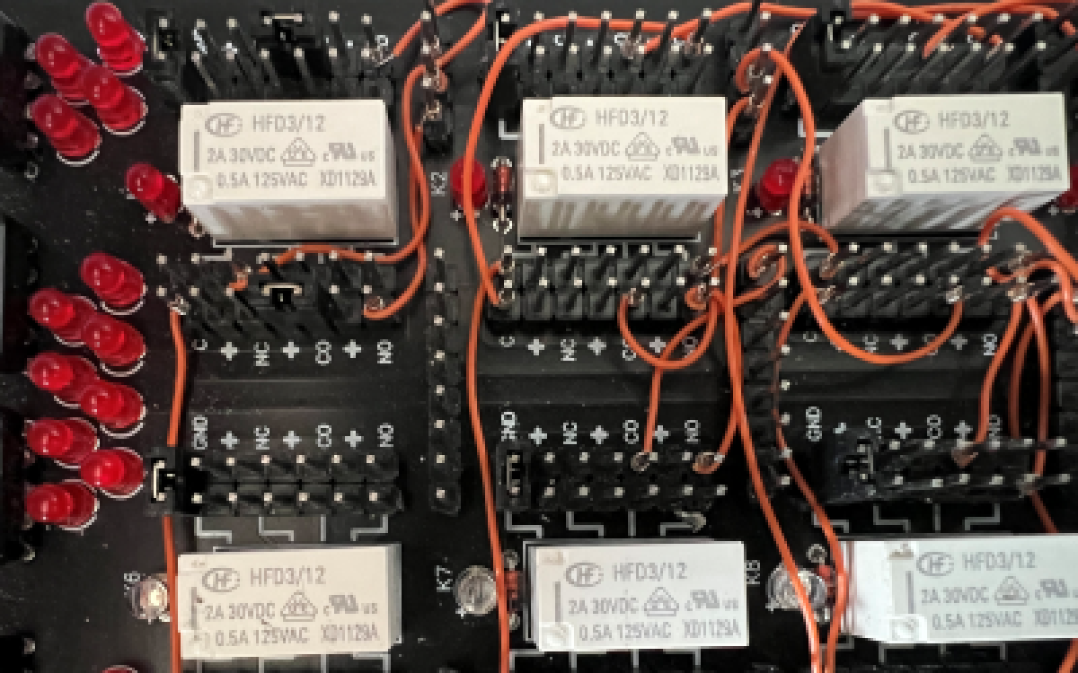
- Everything to do with the core computing functions of the machine has to be done by relay’s (except Memory - see below).
- Diodes can be used to stop back-feeding signals but at a minimum.
- LED’s are allowed for monitoring purposes on the card’s - the more blinkin’ lights the better!
It’s not to say that my machine will be silicon free! - far from…
A RAM chip will be used for main memory. However I want to integrate some other discreet memory devices along side (Relay RAM or Capacitor RAM) just to prove it could work if I had enough time or budget to build a 4096 * 12 bit memory storage by hand! This I feel is an honourable compromise. If I’m going to
cheatcompromise on the RAM - I might as well make the most of it! So my plan will be to use a microcontroller (with wifi) for the RAM. In normal operation the microcontroller will function as basic RAM - implemented as many others have done. However it will also give me the ability to write a debugging interface. The goal will be to view, edit, load and save the memory from a terminal browser or telnet session etc.A Diagnostic card is also planned that will be able to view the busses and manipulate the key control lines. Based on a wifi Enabled microcontroller. Again useful for diagnostics as it’s being built but would also serve another purpose as the ultimate goal would be to put this computer ‘on the net’ so people could write their own programs and run them remotely!
Finally no electronics project would be complete without a ‘555’ timer! So their will be a second clock source built around one of these - just to annoy the purists! Seriously, this will serve a dual purpose, the relay’s that drive the clock will have to cope with a lot of cycles and I am worried about wearing these out. Again I feel having and using a digital clock is acceptable providing that a 100% Relay based clock is built alongside it and we can swap between the two. The other reason is that I will be able to control the 555 timers speed via a variable resistor, this will make it handy for debugging etc. where I can really slow the clock down if I need to.